
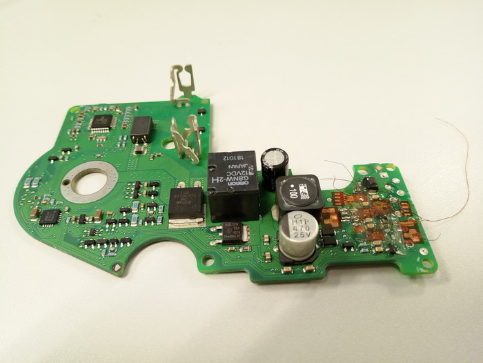
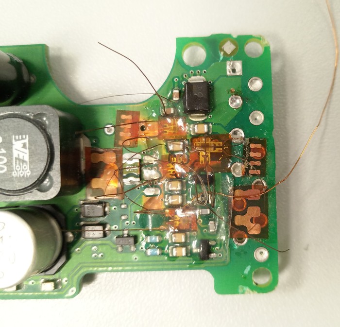
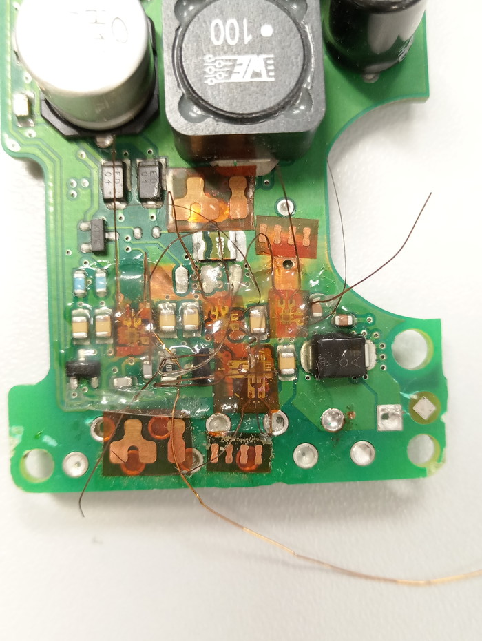
Cracks in Printed Circuit Boards (PCB)
Cracks in PCBs — brittle fractures in solder and even across components, particularly around BGAs — can be induced by in-circuit test fixtures and during assembly, burn-in and testing, system integration, and packaging and shipping. Strain measurements should be made after all design iterations of the PCB, including changes to on-board components, which may alter thermal stress loading. This is especially useful when introducing new solder materials and processes, which may have a different stiffness and introduce a different soldering thermal profile. The miniaturization of consumer electronics — and consequent increase in component density — results in larger thermal stresses, new requirements for surviving repeated loadings, and a greater need for impact stress survival. Meeting these specifications requires accurate knowledge of strains in the PCB and on-board components. Strain gage measurement is the quickest, most accurate, and most cost-effective method for identifying strains on a PCB, and can be used in developing loading fixtures and test plans to optimize the testing phase.
The solution is Micro-Measurements WK-Series strain gage (gauge) sensors designed to meet the growing demand for precise, stable, and reliable stress analysis of PCBs, even in harsh environments.
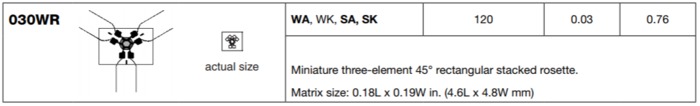
应变片型号 Strain Gage: WK-06-030WR-120
胶水Adhesive: M-Bond 610
保护涂层 Coating: M-Coat C
Checklist: https://www.strainblog.com/content/strain-gage-installation-checklist-printed-circuit-assemblies


Recent comments