
Cutting Edge Technologies – 5G Meets Advanced Sensors Technology.
5G may be the latest buzz word in communications technology, but the question of reliability remains the same. Modern electronics must survive temperature, humidity, impact, force, vibration and occasional misuse. Smaller, higher-density devices become more vulnerable to some of these failure modes – if you’ve ever accidentally sat on a smartphone you’ll understand this well!
Even under perfect conditions devices can fail, and this can be a function of the manufacturing processes, from component placement, ICT (In Circuit Test), depanelling (separating small PCBAs from a lager panel), assembly, packaging and handling.
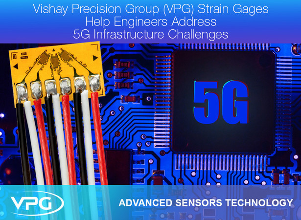
High-speed 5G wireless technology is pushing the design limits. Smaller, flexible PCBs and narrow tracks impose challenges essential to miniaturising this new technology. This revolution in IIOT and industry 4.0 with 5G enables integration into autonomous vehicle infrastructure, network equipment, electronic devices and data transmission networks including industrial and consumer applications such as mobile phones.
PCBs designed for 5G applications will require a new mix of analog and digital components capable of operating at very high frequencies and data rates, whose reliability and efficiency can only be guaranteed through effective thermal and mechanical stress tests .
Strain gauges are the primary tool for evaluating these processes to ensure that the device does not see any input that could initiate a micro-facture. These so-called latent failures mean that a device will work perfectly well until some minor event causes the fracture to propagate. Premature failure can lead to significant warranty claims or loss of customer confidence.
The continuing miniaturisation means that the testing technology needs to keep up. VPG Micro-Measurements have developed our Advanced Sensors Technology from electronic component manufacturing processes to revolutionise the way strain gauges are made. This enables ultra-miniature sensors to be made whilst maintaining performance characteristics of their more traditional ancestors.
Our latest gauges for PCBA testing includes miniature stacked rosettes down to 5.1mm diameter, and a planar rosette with 0.36mm grids in a 3-element rectangular form (0-45-90°) with a footprint of only 2 x 4mm, making this the smallest strain gauge rosette available. With many options of gauge configuration and leadwire/flex connections we can provide sensors for location on even the smallest high-density PCBAs for class-leading test capabilities.
We also manufacture foil temperature sensors. These have high contact area and virtually zero thermal mass to enable accurate tracking of even the fastest temperature transients – ideal for thermal shock testing. In combination with our gauge capable of surviving solder reflow operations this enables testing of even the most extreme conditions that electronics are capable of withstanding.
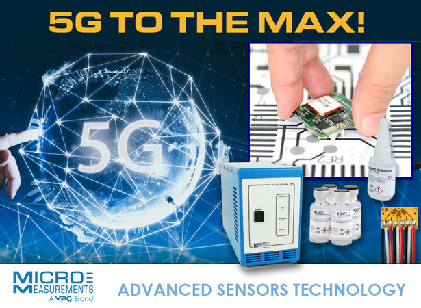
Connected to one of our StrainSmart data acquisition systems with integrated PCBA reports to IPC/JEDEC 9704A, VPG Micro-Measurements are a complete 1-stop shop for all your PCBA testing needs.
This is all backed up by our unrivalled technical support with experts in strain measurement technology and testing. Reach out to your local contact for further information!
Cutting edge technologies – 5G meets Advanced Sensors Technology.
How To Test a PCBA (Printed Circuit Board Assembly).
Easy Way How to Test Printed Circuit Board (Advanced Sensors Technology).
Printed Circuit Board Testing Methods for PCB Design.
Strain Gauge Installation on Printed Circuit Board (PCB).
Want to join an engaged community
of fellow engineers?
Here’s how to connect with the StrainBlog community:
• Subscribe to StrainBlog.
• Watch MM StrainBlog videos on YouTube.
• Follow StrainBlog on Twitter.
• Connect with StrainBlog Editor in Chief Yuval Hernik Bar on LinkedIn.


Recent comments